Multimode interference (MMI) coupler
A power splitter or combiner made of a wide multimode waveguide section between single-mode access waveguides. The modes excited by the input interfere and form single or multiple images of it at lengths set by the beat length L_π = 4n_rW_e²/(3λ₀). A silicon 1×2 splitter 3 µm wide is 8.3 to 8.6 µm long; MMIs are broadband and tolerant of fabrication, but give fixed split ratios.
A multimode interference (MMI) coupler is a power splitter or combiner made of a wide waveguide section that guides many transverse modes, with narrow single-mode waveguides attached at its input and output ends. Light entering through an input waveguide excites the modes of the wide section, which travel at slightly different phase velocities; at certain lengths their interference rebuilds the input field as one image or as several images, the self-imaging effect, and output waveguides placed at those images collect the light. MMIs are the usual 1×2 and 2×2 splitters of photonic integrated circuits, because their splitting holds over a wide band and tolerates errors in fabrication. Soldano and Pennings set out the design rules in 1995.
Self-imaging and the beat length
The propagation constants of the lateral modes of a wide section are spaced almost quadratically with mode number, so their relative phases repeat after a characteristic distance, the beat length of the two lowest modes:
where is the effective index of the slab from which the section is cut, the free-space wavelength and the effective width, the physical width plus the penetration of the modes into the cladding of index . For the TE mode of a silicon slab, whose electric field points across the width and meets the side walls at normal incidence, ; when the field runs along the walls, as for TM, the factor drops out. For a 220 nm silicon slab at 1550 nm, = 2.848 in oxide, and a section 3 µm wide has = 3.05 µm and = 22.8 µm; the two lowest modes of the full cross-section, computed with a mode solver, give 22.6 µm. The section guides ten lateral modes.
Where the images form depends on which modes the input excites, which in turn depends on where the input sits (Bachmann, Besse and Melchior):
- General interference: an input anywhere across the width excites all the modes, and images form at . This gives couplers, including the 2×2 at .
- Paired interference: inputs at one third and two thirds of the width leave every third mode unexcited, and the images form three times sooner, at ; a 2×2 coupler then needs only .
- Symmetric interference: a centered input excites only the even modes, and images form at , spaced apart. This is the usual splitter.
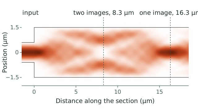
Computed intensity, seen from above, in a 3 µm silicon section fed at its center through a 1.2 µm access waveguide at 1550 nm (TE), from its ten guided modes. Two images form at 8.3 µm, where a 1×2 splitter ends, and the input is rebuilt at 16.3 µm, a few percent short of the paraxial = 8.6 µm and = 17.1 µm. The width is drawn at twice the scale of the length, and the shading follows the 0.7 power of the intensity; the dashed lines mark the lengths of best coupling into output waveguides.
Design lengths in silicon
Computed for a 220 nm silicon slab in oxide at 1550 nm, TE polarization:
| Device | Section width | Interference | Length | Port spacing |
|---|---|---|---|---|
| 1×2 splitter | 3 µm | Symmetric | 8.6 µm | 1.53 µm |
| 2×2 coupler | 3 µm | Paired | 11.4 µm | 1.02 µm |
| 2×2 coupler | 3 µm | General | 34.2 µm | 1.53 µm |
| 1×4 splitter | 6 µm | Symmetric | 16.8 µm | 1.51 µm |
| 4×4 coupler | 6 µm | General | 67.3 µm | 1.51 µm |
| 1×8 splitter | 12 µm | Symmetric | 33.4 µm | 1.51 µm |
Wider sections are used for more outputs so that the access waveguides stay far enough apart not to couple to each other, and because grows as , doubling the width nearly quadruples the beat length. The formula is a paraxial approximation, and designs start from it and are then refined by numerical simulation, which also sets the tapers that widen the access waveguides where they meet the section to make the images sharper. In a two-dimensional modal calculation for the 3 µm section, the best pair of images forms at 8.3 µm with 1.2 µm access waveguides, where 99% of the power reaches the two outputs, and at 7.9 µm with 0.8 µm guides, where 94% does: a narrower input excites more of the higher modes, whose propagation constants depart furthest from the quadratic spacing.
Simulation methods for MMIs and other passive devices are compared in Choosing a Photonics Simulation Method.
Splitting, phase and loss
A symmetric splitter divides the light equally, dB into each output (3.0 dB for two, 9.0 dB for eight), and its outputs are in phase for = 2. The two outputs of a 2×2 coupler are 90° apart in phase, as in a directional coupler, and a 4×4 MMI provides the 90° relations of a coherent receiver's optical hybrid. Used in reverse, a MMI combines light coherently only when the inputs arrive with the right phases; light from independent sources is combined with only of each passing, 10.8 dB for the twelve lasers of a DFB array. Excess loss beyond the ideal split comes from imperfect images, since only a finite number of modes are guided and the paraxial phase relation is not exact, and from reflections at the flat ends of the section.
Tolerances and bandwidth
Because scales as , a width error of 50 nm in a 3 µm section changes the self-imaging length by 3.3%, which moves the images of the 1×2 splitter by 0.3 µm along its length; the split of a symmetric 1×2 stays at 50:50 regardless, by symmetry, and the error appears as a small excess loss. Across the C-band, 1530 to 1565 nm, of the 3 µm section changes by ±1.4%, computed with the dispersion of silicon and silica, so an MMI keeps its splitting over a band much wider than a directional coupler, whose 50:50 point holds over only ±5 to 10 nm. The TE and TM modes of a silicon slab have very different effective indices and image at different lengths, so a silicon MMI is designed for one polarization.
MMI or directional coupler
| MMI coupler | Directional coupler | |
|---|---|---|
| Split ratio | Fixed by the geometry, usually equal | Any ratio, set by the coupling length |
| Bandwidth | Wide | Narrow for a 50:50 split |
| Sensitivity to fabrication | Low: width enters as | High: coupling depends exponentially on the gap |
| Footprint | Tens of µm for small | Tens of µm, plus bends |
| Small tap ratios, such as 1% | Awkward | Natural |
MMIs are the usual splitters at modulator inputs, in the arms of Mach-Zehnder interferometers, in coherent receivers, and in the trees that feed optical phased arrays. A Y-branch is the other common 1×2 splitter.
Common questions
How does an MMI coupler work?
The input light excites many modes of a wide waveguide section. Because their propagation constants are spaced quadratically, their phases realign at particular lengths, where the input field reappears as one or several images; output waveguides placed at the images collect the light.
How long is an MMI coupler?
It scales with the square of the width. In 220 nm silicon at 1550 nm, a 3 µm-wide section has a beat length of 22.8 µm from the formula. A center-fed 1×2 splitter then needs 8.6 µm (8.3 µm in a full modal calculation) and a paired-interference 2×2 coupler 11.4 µm; a 6 µm-wide 1×4 splitter needs 16.8 µm.
What is the difference between an MMI and a directional coupler?
An MMI divides light by self-imaging in one wide section and gives fixed ratios, usually equal, over a wide band with low sensitivity to fabrication. A directional coupler transfers power between two closely spaced waveguides and can give any ratio, but its split depends strongly on the gap and the wavelength.
What is the phase relation between the outputs of a 2×2 MMI?
The two outputs are 90° apart in phase, as in a directional coupler. A 4×4 MMI gives the 90° phase relations needed in a coherent receiver's optical hybrid.
References: L. B. Soldano and E. C. M. Pennings, "Optical multi-mode interference devices based on self-imaging: principles and applications," Journal of Lightwave Technology 13, 615 (1995). M. Bachmann, P. A. Besse and H. Melchior, "General self-imaging properties in N × N multimode interference couplers including phase relations," Applied Optics 33, 3905 (1994). L. Chrostowski and M. Hochberg, Silicon Photonics Design (Cambridge University Press, 2015).