Free-carrier absorption (FCA)
Light absorbed by free electrons and holes in a semiconductor. Silicon at 1550 nm with 10¹⁸ cm⁻³ of each: 14.5 cm⁻¹, 6.3 dB/mm. Soref-Bennett formula, materials, mitigation.
Free-carrier absorption (FCA) is the absorption of light by electrons already in the conduction band and holes already in the valence band. A carrier takes up the photon's energy by moving to a higher state within its own band, so light below the bandgap is absorbed and no electron-hole pair is created. In silicon at 1550 nm each electron adds cm² of absorption cross-section and each hole cm² (Soref and Bennett), so cm⁻³ of each absorbs 14.5 cm⁻¹, or 6.3 dB/mm. FCA is the loss that comes with the plasma dispersion effect, the index change made by the same carriers. It adds loss to every carrier-based silicon modulator and to the internal loss of laser diodes, and with two-photon absorption it limits the power a silicon waveguide can carry.
How free carriers absorb light
A photon carries almost no momentum, while a move to a higher energy in the same band needs a change of crystal momentum. The transition therefore takes place only when a phonon or an ionized impurity supplies the difference at the same moment, and the strength of the absorption depends on how the carriers scatter. Calculations for the separate mechanisms give an absorption that grows with wavelength as about for scattering by acoustic phonons, for optical phonons and to for ionized impurities (Pankove, ch. 3). The energy ends as heat, as the excited carrier relaxes back to the band edge by emitting phonons.
Free-carrier absorption formula
For electron density and hole density , the absorption coefficient is the sum of the two carrier contributions:
where and are absorption cross-sections, measured for each material and wavelength. The loss is linear in density while the cross-sections stay fixed; the more recent silicon fits carry a slightly higher power of density.
The classical Drude model gives the cross-sections in closed form. The carriers are driven by the optical field and damped by collisions with a mean time between them. At optical frequencies , about 50 for electrons in silicon doped to cm⁻³ at 1550 nm, and the absorption coefficient is
with the conductivity effective masses, the mobilities and the refractive index. Carriers that scatter more, with lower mobility, absorb more, since every absorption needs a scattering event. For silicon the formula falls short of measurement: with , a low-field mobility of 270 cm²/Vs for silicon doped to cm⁻³ and , it gives 2.0 cm⁻¹ for cm⁻³ electrons at 1550 nm, about a quarter of the measured 8.5 cm⁻¹. Silicon device work uses the measured cross-sections.
Free-carrier absorption in silicon
Soref and Bennett derived the standard relations from measured absorption spectra of doped silicon. At 1550 nm,
with and in cm⁻³; at 1310 nm the coefficients are and cm². Injecting cm⁻³ of electrons and holes at 1550 nm gives 14.5 cm⁻¹, or 63 dB/cm, and a waveguide doped n-type to cm⁻³ loses 0.85 cm⁻¹, or 3.7 dB/cm.
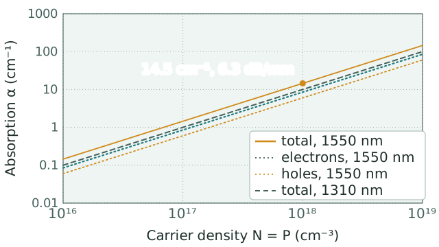
Silicon free-carrier absorption against carrier density with , from the Soref-Bennett cross-sections above at 1550 nm and their 1310 nm values, and cm². Absorption is linear in density, so every line has unit slope on these axes.
Between 1.3 and 2 µm the silicon values grow roughly as . The 1310 nm coefficients are 0.71 (electrons) and 0.67 (holes) of those at 1550 nm. At 2 µm the 2011 fits of Nedeljkovic, Soref and Mashanovich give 15.5 cm⁻¹ for cm⁻³ of electrons and 8.6 cm⁻¹ for holes, 1.72 and 1.61 times their own 1550 nm values. Mid-infrared silicon photonics escapes two-photon absorption beyond 2.2 µm, where two photons no longer span the 1.12 eV bandgap, but each carrier present absorbs more there.
The Plasma Dispersion Calculator gives the index change and loss of doped or injected silicon at 1310, 1550 and 2000 nm from both sets of relations, and the decibels a π phase shift costs.
Other semiconductors
Holes in III-V semiconductors such as InGaAsP also absorb by intervalence-band absorption, in which a hole moves from the heavy-hole band to the split-off band. The transition is between two valence bands at the same crystal momentum, so it needs no phonon. Henry and co-workers analyzed its effect on the temperature behavior of InGaAsP lasers in 1983. Because holes absorb this way, InP-based lasers keep the p-doping low near the active layer, and high-power designs use asymmetric waveguides that shift the mode toward the n side.
In germanium, the heavy n-type doping used with tensile strain to obtain optical gain at 1.55 µm brings free-carrier loss that the gain has to overcome (Liu et al., 2007).
Where free-carrier absorption matters
- Silicon modulators. The carriers that change the index in carrier-injection and carrier-depletion phase shifters also absorb, so a larger index change costs more loss. Injecting cm⁻³ of each carrier at 1550 nm changes the index by , so a π phase shift takes 257 µm and adds 1.62 dB of FCA to the modulator's insertion loss, with the mode wholly in the injected region.
- Laser diodes. The doped cladding layers carry free carriers, and the part of the mode that extends into them is absorbed. Doping is graded down toward the active region, and the cladding is made thick enough to keep the mode off the heavily doped contact layer (see carrier confinement). FCA is part of the internal loss in the threshold condition of the modal gain entry.
- Semiconductor optical amplifiers. The injected carriers that provide gain also absorb, so the internal loss of an SOA rises with carrier density and offsets part of the gain.
- Photodiodes. A photon absorbed by a free carrier in a doped contact layer creates no electron-hole pair, so doped layers in the light path lower the quantum efficiency and with it the responsivity.
- Silicon waveguides at high power. Two-photon absorption creates electron-hole pairs at a rate proportional to , and the carriers absorb until they recombine. The steady-state carrier density, and with it the FCA coefficient, grows as , so the power lost to FCA grows as . A reverse-biased p-i-n junction across the waveguide sweeps the carriers out and shortens their lifetime; it made the first continuous-wave silicon Raman laser possible (Rong et al., 2005).
Reducing the loss in silicon modulators
- Holes rather than electrons. At cm⁻³ and 1550 nm, holes give 3.4 times as much index change per unit of absorption as electrons in the Soref-Bennett relations: for 6.0 cm⁻¹, against for 8.5 cm⁻¹.
- Contact doping away from the mode. The heavily doped regions under the metal contacts sit in the slab, away from the mode, with moderate doping where the mode overlaps the junction. Heavier doping lowers the series resistance and raises the speed but adds loss.
- Depletion instead of injection. A depletion phase shifter only sweeps carriers out of a moderately doped junction, so its loss is set by that doping rather than by injected densities of cm⁻³. It is also faster, since no carrier lifetime limits it, but needs a longer phase shifter for the same phase.
- Resonators. A microring modulator shifts the resonance of its ring resonator with a small index change in a device tens of micrometers around, so the light meets far fewer carriers than in a Mach-Zehnder phase shifter millimeters long.
Measuring free-carrier absorption
The cross-sections come from transmission measurements on samples of known doping, or from pump-probe measurements in which a pump pulse creates a known carrier density and a probe at the wavelength of interest records the added absorption. In waveguide devices the carrier-induced loss is found from the change in transmission with forward current through a p-i-n phase shifter, or from the nonlinear loss at high power, fitted with both two-photon absorption and FCA, which also yields the effective carrier lifetime.
Common questions
What is free-carrier absorption?
The absorption of light by free electrons and holes already present in a semiconductor's bands. The carrier moves to a higher energy in its own band, with a phonon or impurity supplying the momentum, so light below the bandgap is absorbed and no electron-hole pair is created.
How large is free-carrier absorption in silicon at 1550 nm?
cm⁻¹ (Soref and Bennett). cm⁻³ of each carrier gives 14.5 cm⁻¹, 63 dB/cm; cm⁻³ of electrons alone gives 0.85 cm⁻¹, 3.7 dB/cm.
How does free-carrier absorption depend on wavelength?
It grows with wavelength as , with between about 1.5 and 3.5 depending on how the carriers scatter. In silicon between 1.3 and 2 µm the measured values follow roughly .
What is the difference between free-carrier absorption and two-photon absorption?
Two-photon absorption takes two photons at once to lift an electron across the bandgap, creating an electron-hole pair at a rate proportional to . Free-carrier absorption is one photon taken up by a carrier that is already free, at a rate proportional to the carrier density. In silicon at high power the first supplies the carriers for the second.
How is free-carrier absorption related to the plasma dispersion effect?
They are the absorptive and refractive parts of the same carrier response. Soref and Bennett obtained the index change in silicon by applying the Kramers-Kronig relations to measured absorption spectra of doped silicon, so a phase shifter that changes the index with carriers always pays this loss.
References: Soref and Bennett, "Electrooptical effects in silicon," IEEE J. Quantum Electron. 23, 123 (1987); Nedeljkovic, Soref and Mashanovich, "Free-carrier electrorefraction and electroabsorption modulation predictions for silicon over the 1–14 µm infrared wavelength range," IEEE Photonics J. 3, 1171 (2011); Pankove, Optical Processes in Semiconductors (Dover, 1971), ch. 3; Henry, Logan, Merritt and Luongo, "The effect of intervalence band absorption on the thermal behavior of InGaAsP lasers," IEEE J. Quantum Electron. 19, 947 (1983); Liu et al., "Tensile-strained, n-type Ge as a gain medium for monolithic laser integration on Si," Opt. Express 15, 11272 (2007); Rong et al., "A continuous-wave Raman silicon laser," Nature 433, 725 (2005).