Apodization (apodized gratings and apodizing filters)
Tapering the strength of a grating, the transmission of a pupil or the weight of an interferogram smoothly toward its ends, so that the sidelobes a sharp edge produces disappear. Used in Bragg gratings, grating couplers and WDM filters, in imaging, and in Fourier-transform spectroscopy.
Apodization means tapering a structure's strength smoothly toward zero at its edges, so that the sidelobes a sharp edge produces disappear, at the cost of a wider main response. It goes by three names: apodized gratings (fiber Bragg gratings, grating couplers and WDM filters, whose coupling strength is tapered along their length), apodizing filters or apodizers in imaging (pupil masks whose transmission falls toward the rim), and apodization functions in Fourier-transform spectroscopy (weights applied to the interferogram before the transform).
The word is Greek for "removing the feet", and the feet are the sidelobes that any sharply bounded structure produces in the conjugate domain: the rings of an Airy pattern around a star image, the ripples beside the spectral line of a Fourier-transform spectrometer, the sidelobes on either side of a Bragg grating's reflection peak. A hard edge in space or time becomes a in angle, frequency or wavelength, and the first sidelobe of a response sits only 13.3 dB below the peak. Replacing the hard edge with a gradual one trades a wider main lobe for sidelobes tens of decibels lower. The technique is the same in every field; what differs is the physical quantity that is tapered.
Apodization functions and sidelobe levels
Any window function of digital signal processing serves as an apodization profile, and the classic tabulation by Harris gives their figures of merit. The main-lobe width is quoted relative to the untapered rectangle.
| Profile | Highest sidelobe | 3 dB main-lobe width | Where it is used |
|---|---|---|---|
| Rectangular (no apodization) | −13.3 dB | 1.00 | the default; narrowest response |
| Triangular (Bartlett) | −26.5 dB | 1.44 | FTIR spectroscopy, the standard "triangular apodization" |
| Hann (raised cosine) | −31.5 dB | 1.62 | general purpose, gratings, spectral analysis |
| Hamming | −42.7 dB | 1.46 | filters that need low near-in sidelobes |
| Blackman | −58.1 dB | 1.89 | narrowband notch and add-drop filters |
| Gaussian, truncated at 3σ | about −55 dB | about 1.7 | fiber Bragg gratings, grating couplers |
| Tukey (cosine-tapered) | adjustable | adjustable | tapers only the ends; keeps most of the length at full strength |
| Kaiser | adjustable | adjustable | the optimum trade of sidelobe level against width for a given length |
For a weak grating the reflection spectrum is the Fourier transform of the coupling-coefficient profile , so the numbers apply directly; for a strong grating the coupled-mode equations have to be solved, the bandwidth grows with and the sidelobe suppression is somewhat less than the window function alone promises, but the ordering of the profiles is unchanged.
Apodized gratings
A uniform Bragg grating, whether a fiber Bragg grating, a DBR mirror or a sidewall grating in silicon, reflects a -like spectrum whose sidelobes leak into adjacent WDM channels, put ripple on a laser mirror's reflectivity, and, in chirped gratings used as dispersion compensators, produce group-delay ripple that penalizes the link. Apodizing the index modulation removes them. Three things have to be got right. The taper must be applied to the modulation depth, not to the average index: if the average index also rises toward the grating center the local Bragg wavelength varies along the length, the grating chirps itself, and a Fabry-Pérot-like structure of sidelobes appears on the short-wavelength side. Fiber gratings written with a phase mask are therefore "pure-apodized" by a second exposure that keeps the mean index constant. The taper must be realizable: in a silicon sidewall grating the strength is set by the corrugation width or the filling factor, and the weak ends of a Gaussian profile call for corrugations of a few tens of nanometers, at or below the resolution of deep-UV lithography, which is why designs stop the taper at a minimum feature and accept the residual sidelobe. And the length must be increased to hold the bandwidth, since a Gaussian taper roughly halves the effective length of the grating.
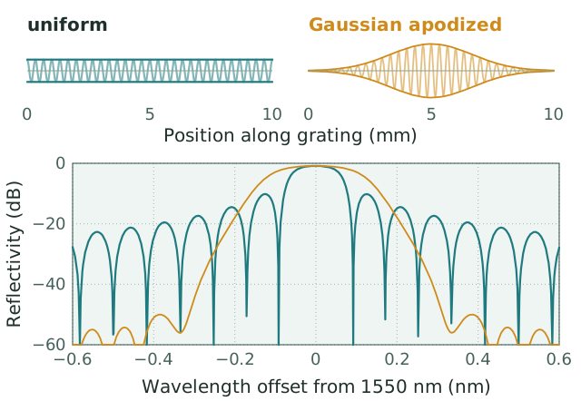
Coupled-mode reflection spectra of two 10 mm fiber Bragg gratings at 1550 nm () with the same integrated coupling, , and therefore the same 82 % peak reflectivity. The uniform grating's highest sidelobe is 9.3 dB below the peak, above the weak-grating 13.3 dB; the Gaussian (, cut at ±3σ, constant mean index) leaves residual lobes 49 dB down and widens the half-maximum width from 0.12 to 0.23 nm. Fringes are not to scale.
| Method | What is varied | Where |
|---|---|---|
| Corrugation width or filling factor | tooth width | silicon and silicon nitride sidewall gratings, contra-directional couplers |
| Corrugation depth | etch depth along the length | rarely, since it needs a gray-scale or multi-step etch |
| Duty cycle with fixed period | fraction of the period etched | grating couplers |
| Waveguide separation | gap between the grating and the bus | ring and contra-directional coupler filters |
| Exposure dose along the fiber | ultraviolet fringe visibility | fiber Bragg gratings, with a mean-index correction |
| Phase-mask with variable diffraction efficiency | mask pattern | fiber Bragg gratings in volume production |
Apodized grating couplers
A uniform grating coupler radiates a field that decays exponentially along its length, and the overlap of a decaying exponential with the Gaussian mode of a fiber cannot exceed about 80 %, a loss of 1 dB before anything else is counted. Apodizing the grating, weak at the input end and strong further along, shapes the radiated field into a Gaussian and recovers most of that decibel; in silicon the taper is a duty cycle rising from roughly 0.3 to 0.6 or an etch depth that increases along the grating, and the best apodized couplers reach about 1 to 1.5 dB of coupling loss where uniform ones sit at 3 to 4 dB.
Apodization filters in imaging
In imaging the apodizer is a pupil mask whose transmission falls smoothly toward the edge. Apodized-pupil Lyot coronagraphs use one to suppress the Airy rings of a star so that a planet a millionth as bright can be seen a few diffraction widths away, at the cost of a broader core and lost throughput. The apodization filter of a smooth-transition-focus camera lens is the same object with a different purpose: a radially graded neutral density element that turns the hard-edged out-of-focus disk into a soft one.
Apodization in FTIR spectroscopy
In Fourier-transform spectroscopy the apodization function is a weight applied to the interferogram before the transform. The finite scan is a rectangular truncation, which gives every line a sinc shape with a negative sidelobe 22 % of the peak on either side; triangular apodization turns the line shape into a sinc², whose largest sidelobe is 4.7 % and positive, and the Happ-Genzel (a Hamming-type window) and Norton-Beer functions offer other trades between resolution and ringing. In each case the trade is the one the table quantifies: sidelobes fall, the main lobe widens, and some energy or resolution is given up for a cleaner response.
Common questions
What does apodization mean?
Tapering the strength of a grating, the transmission of a pupil or the weight of an interferogram smoothly toward zero at the edges, so that the sidelobes a sharp edge produces disappear. The name is Greek for "removing the feet", and the price is a wider main lobe.
What is an apodization filter?
In imaging, a pupil mask whose transmission falls toward the rim. Coronagraphs use one to suppress a star's Airy rings, and smooth-transition-focus camera lenses use a radially graded neutral density element to soften out-of-focus highlights.
What is an apodized grating?
A Bragg grating, grating coupler or WDM filter whose coupling strength is tapered along its length, usually with a Gaussian or raised-cosine profile, so that its spectrum has no sidelobes leaking into neighboring channels. The mean index has to stay constant along the grating, or the grating chirps itself.
Which apodization function suppresses sidelobes most?
Among the fixed profiles in the table, Blackman (−58.1 dB) and a Gaussian truncated at 3σ (about −55 dB) go lowest, with main lobes 1.7 to 1.9 times as wide as the untapered one. A Kaiser profile gives the best trade between sidelobe level and width for a given length.
Does apodization reduce resolution?
Yes. Every profile widens the main lobe, triangular by a factor of 1.44 and Hann by 1.62 at the 3 dB points, which in a spectrometer means coarser resolution and in a grating a wider reflection band for the same length.
References: F. J. Harris, "On the use of windows for harmonic analysis with the discrete Fourier transform," Proceedings of the IEEE 66, 51 (1978). A. Othonos and K. Kalli, Fiber Bragg Gratings: Fundamentals and Applications in Telecommunications and Sensing (Artech House, 1999), chapter 4. B. Malo, S. Thériault, D. C. Johnson, F. Bilodeau, J. Albert, and K. O. Hill, "Apodised in-fibre Bragg grating reflectors photoimprinted using a phase mask," Electronics Letters 31, 223 (1995). D. Taillaert, P. Bienstman, and R. Baets, "Compact efficient broadband grating coupler for silicon-on-insulator waveguides," Optics Letters 29, 2749 (2004). L. Chrostowski and M. Hochberg, Silicon Photonics Design (Cambridge University Press, 2015), chapters 4 and 5. R. Soummer, "Apodized pupil Lyot coronagraphs for arbitrary telescope apertures," Astrophysical Journal 618, L161 (2005).